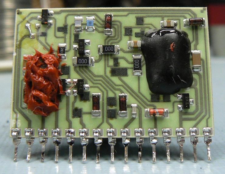
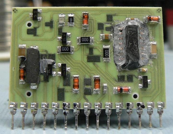
Eric Shultz was able to remove the potting material from a number of HC1010 and HC1011 modules. The resultant schematic below shows that the control of the amplifier rail voltage is not nearly as complex as was imagined. A UC3842A fixed-frequency, current-mode controller IC drives the FETs in the Digital Converter in response to the demands fed to it by the Amplifier Board's AMP-LEVEL signal.

Schematic diagram of Indigo BASH HC1010 / HC1011 Module
|
UC3842A Operation
The UC3842A operates as a current-mode controller, whereby output switch conduction is initiated by the oscillator and terminated when the peak inductor current reaches the threshold level established by the error amplifier. Thus the error signal controls the peak inductor current on a cycle-by-cycle basis. The current-sense-comparator/PWM-latch configuration used ensures that only a single pulse appears at the output during any given oscillator cycle.
Oscillator
The oscillator frequency is programmed by the values selected for the timing components RT and CT. Capacitor CT is charged from the 5.0 V reference through resistor RT to approximately 2.8 V and discharged to 1.2 V by an internal current sink. During the discharge of CT, the oscillator generates an internal blanking pulse that causes the output to be in a low state, thus producing a controlled amount of output deadtime.
Error Amplifier
The error amplifier non-inverting input is internally biased at 2.5 V. The FET gate-drive output voltage is divided down as described later and
monitored by the inverting input. An external loop compensation output connects from the error amplifier output to the inverting input. Output of the error amplifier goes to the current-sense comparator.
Current-Sense Comparator and PWM Latch
The inductor current of the buck converter is converted to a voltage by the ground referenced FET source resistor. This voltage is monitored by the I-Sense input and
compared to the error amplifier output level. The peak inductor current is controlled by the voltage at the VFB input to the error amplifier.
Control of the UC3842A
Overview
Here is how the UC3842A works. A R/C oscillator sets a period, and a latch turns on at the beginning of the period. The latch turns off when the voltage accross the driven FET source resistor reaches a threshold voltage. The threshold is established by a voltage, VFB, at the input to an error amplifier. VFB is derived by comparing the AMP-LEVEL signal (desired voltage) from the Amplifier Board to the floating rail voltages (actual voltage) applied to the Amplifier Board.
FB-IN
As the rail voltage increases, the voltage at this input increases and the current through the 5401 transistor increases. This raises the voltage at the VFB terminal of the UC3842A and lowers the current-sense threshold thus decreasing the FET gate-drive pulse width. When the drive pulse goes low, a 20.5K resistor on the transistor emitter is pulled low through a 4148 diode. This decreases the current through the 5401 transistor and provides hysterisis for the FET switching.
AMP-OC
If there is an over-current event in one of the Amplifier Boards, the board produces a positive logic output. A positive logic voltage from any Amplifier Board raises the VFB voltage to the UC3842A and cuts the drive to the FET gates to reduce the current to the Amplifier Board. When the over-current event is corrected, the rail voltage is restored to normal without the need for resetting.
FB-OUT
A connection to the center of the voltage divider providing the control voltage to the UC3842A error amplifier is brought out on this pin. An external resistor to ground connected to this pin becomes part of the lower leg of the voltage divider string and can adjust the center point and control range of the Digital Converter.
AMP-LEVEL
This is the lower leg of the voltage divider providing the control voltage to the UC3842A error amplifier. It comes from a peak audio level detector on each channel's Amplifier Board. The board having the highest audio level sets the level for all the Amplifiers rail voltage. The AMP-LEVEL voltage is compared to the -15V reference voltage by a 5401 transistor and adjusts the drive to a 4401 transistor. The 4401 transistor is the bottom leg of the divider string and sets the desired VFB voltage to the UC3842A
I-SENSE
The voltage across the Digital Converter FET source resistor is sensed to reset the latch when the FET current reaches its peak value.
DRIVE
This is the voltage that turns on the Digital Converter FETs in response to all of the above.
Module Versions
Some early V4.1 units may have used an HC1010 module instead of the HC1011, or perhaps some of the late V2-400 used the HC1011. The change over date is not known.