New Version Klipsch Promedia V2.1 Amplifier
Block and Interconnect Diagrams
The most popular (reliable) Promedia got an update: new power supply, integrated circuits replaced discreate components, new design all around.
Will it be as failure prone as the 4.1 and 5.1?
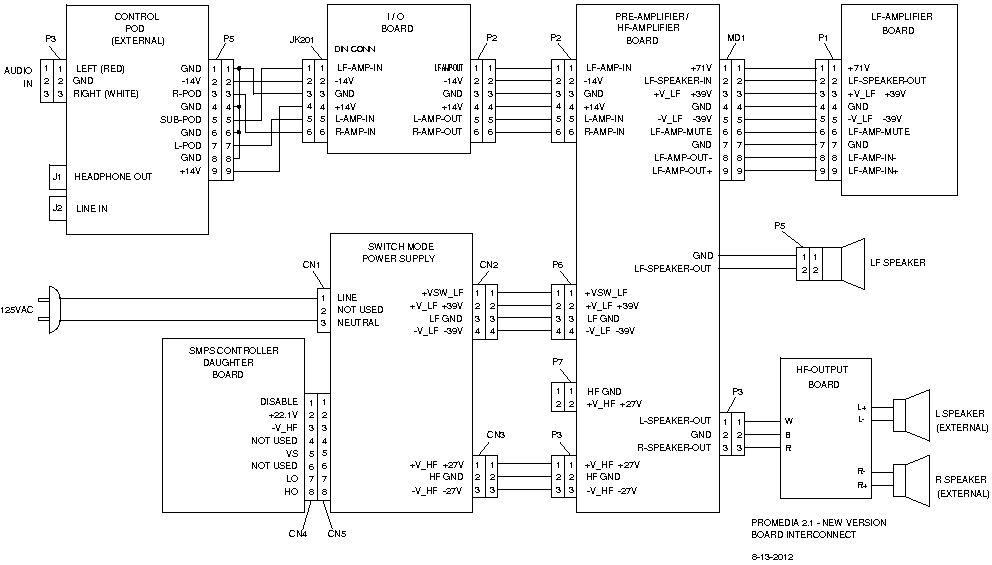
The new Klipsch ProMedia 2.1 computer speaker system, like its predecessor, has two satellite speakers with a control pod on one of them, and a sub woofer that has the amplifier circuits inside with the speaker.
A headphone jack and a line-in jack are included in the control pod together with the main- and sub-woofer-volume controls.
The subwoofer has one side-firing 6.5" long-throw fiber composite cone speaker in a bass reflex tuned MDF box. Driving the speaker is a Class A/B amplifier that puts out 50 watts @ 7% THD from 40- to 100-Hz. Maximum burst power is 200 watts @ 10% THD.
At a crossover frequency of 100Hz the satellite speakers kick in. They each have a 0.75" poly compression driver tweeter for frequencies above 5kHz, a 90° x 40° high frequency horn, a 3" long-throw fiber-composite cone woofer in an ABS plastic case. Pumped up by two linear A/B amplifiers, the satellites join the subwoofer to give a total frequency response of 31Hz to 20kHz.
Below are the interconnections for the system. The control pod and the satellite speakers shown are separate units; all other connections are internal to the subwoofer box.
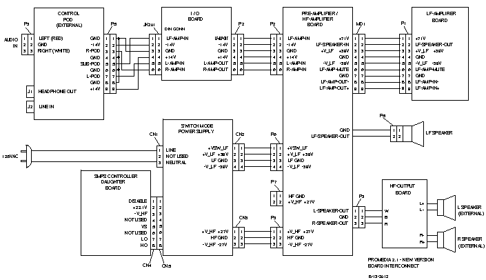
Interconnect diagram of New Version Klipsch Promedia V2.1
|
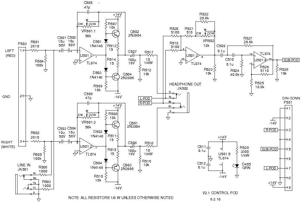
Control Pod
The control pod receives the left and right audio mini-jack input, provides an auxiliary input and headphone output, and mixes the input signals into a summed subwoofer signal. The signal is then buffered by an op amp with a discrete-component output stage (providing a robust headphone amplifier) and then sent to the I/O board through a DIN cable. The signals are also mixed together to create a subwoofer signal with level control, and sent through a high-pass, second-order, Sallen-Key filter before leaving the control pod PCB. When headphones are plugged in the signal is broken and the front channel signal does not leave the control pod PCB.
When the power switch is turned on, a LED glows green. For all three audio signal paths, volume control is produced by changing the amount of feedback around an op amp. Although it works, this is a poor design choice.
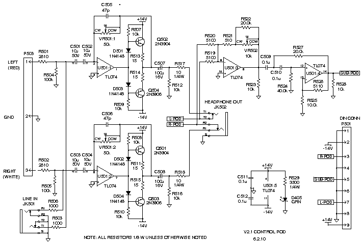
Schematic diagram of Control Pod
|
The diagram below for the V2.1 DIN plug was taken from Klipsch forum postings that I believe are correct. I have not verified it, but I have not found any posts disputing its accuracy. The pin numbers on these diagrams don't conform to the DIN standards.
These diagrams are shown looking at the mating side of the plug pins and not the soldered side.
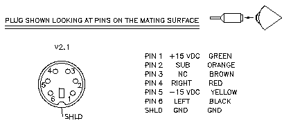
2.1 DIN Plug Wiring Diagram
|
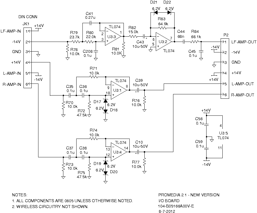
I/O Board
The I/O board receives audio signals for each satellite speaker and sends it through a 2nd order Sallen Key high pass filter. The audio is then AC coupled and sent to the HF amplifiers. The subwoofer signal is low-pass filtered with a second-order, Sallen-Key filter, AC coupled and buffered while having its amplitude nearly halved, and then filtered again by a passive first-order filter before being sent to the LF amplifier (via the HF amplifier PCB).
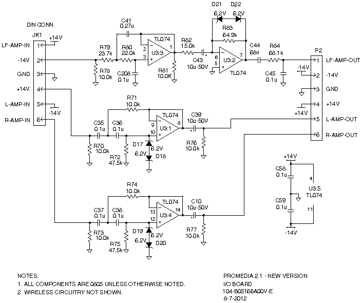
Schematic diagram of I/O Board
|
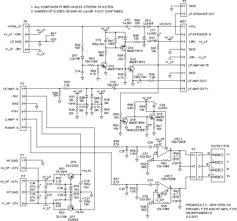
HF Amplifier Board
The HF amplifier board is home to quite a few disparate circuits. It receives audio signals from the I/O board, and the power supply outputs, and it contains the HF amplifiers along with support for the LF amplifier daughterboard. The HF amplifiers are, unfortunately, a downgrade compared with the original PM2.1
Each HF amplifier has a small, passive low-pass filter and is AC coupled to the HF amplifier input. The HF amplifiers are simply an integrated, stereo IC chip amplifier. Resistors R59 and R60 set the gain of the HF amplifiers at almost 27. There is no DC feedback due to C26. Resistor R63 and capacitor C28 form a Zoebel filter on the amplifier output to ensure stability. As in the original PM2.1, the HF amplifier outputs are brought to spring clip terminals on the amplifier module back panel.
There is a clamp circuit designed into the board, but the components are not present, so it is not functional. It would operate as follows if the components were present. The LF amplifier audio signal would pass through the clamp circuit. The threshold would be set by the R37/R38 or R39/R40 resistor dividers. When the peak audio voltage was a diode drop above the threshold set by the resistor dividers, D8 or D9 would conduct and clamp the audio signal level. Resistor R35 would limit current and C12/C13 adjust the attack time of the limiter.
Resistor R36 and capacitor C11 set the gain of the LF amplifier, along with other components on the LF ampamplifier daughterboard.
+VSW_LF, a square wave with an amplitude of ±39V primarily used to generate the LF amplifier rails, is routed to the HF amplifier board to provide two functions: supply a bootstrap voltage for the LF amp and determine the presence of SMPS switching, which controls the amplifier mute circuitry.
Capacitor C15 AC couples +VSW_LF so it can be doubled by D12 and D13. This produces a +71V rail for providing a bootstrap voltage for the gate of the upper output FET of the LF amplifier. This voltage is placed on top of +V_LF, being +33.5V higher, and is stored on C17.
+VSW_LF is rectified by D11 and stored on C14. A voltage here indicates the SMPS is switching; without switching, R43/R44 discharge C14, and mute all amplifiers. A running SMPS turns on Q13 which, after a time delay set by C16 and R45/R47, turns on D10 and Q14. This turns on Q15, which finally enables the LF amplifier and holds off Q18. With Q18 off, D16 charges through R68 and turns on Q19. There is a delay caused by C30 and R69, but eventually Q19's collector moves 6V below +V_HF, turning on the HF amplifier. At this point all amplifiers are un-muted and will stay that way as long as the SMPS supply doesn't stop.
Transistors Q16 and Q17 are the pass transistors for a pair of linear, bipolar regulators which send ±14V the I/O board and control pod.
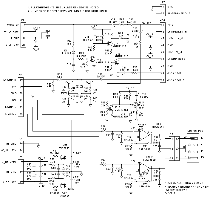
Schematic diagram of HF Amplifier Board
|
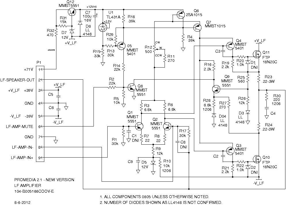
LF Amplifier Board
The LF amplifier is a daughterboard of the HF amplifier board and is a very simple linear amp. It receives ±39V rails, a +71V bootstrap rail, a mute signal, and a differential input (but used single-ended). It delivers a single output.
Transistor Q12 receives the bootstrap voltage, 33.5V above +V_LF, and regulates it with D7 to approximately 12V above +V_LF. Capacitor C7 provides energy storage at the regulator output, and C6 is a quick discharge in case the voltage ever gets below +V_LF. This voltage rail is called +12VHI here, for convenience. The +12VHI is also used to provide a reference voltage to biased various circuits.
Transistors Q1 and Q2 form a usual long-tail diff pair with Q6 biasing this pair of transistors and R12 setting the bias current. The bottom (emitter side) of the differential pair is fixed by D5 and R9/R10. Fixing the bottom side allows either collector to pull low and turn on either the upper or lower output transistor. The output transistors are N-channel FETs, each with a degeneration resistor. This is accomplished by turning on either Q3 or Q4, which applies more than the gate threshold voltage to the FET gates through Q7. Each FET has a gate resistor (R20/R22) and a turn-off resistor (R19/R21). Diodes D1and D2 are not inserted, but were intended to prevent overvoltage on the FET gates.
As on the HF amplifier, R30 and C4 are a Zoebel network for amplifier stability under reactive loads.
An overcurrent condition is created when the voltage across either R23 (positive current) or R24 (negative current) causes Q9 to turn on. With Q9 turned on, the output FETs are prevented from turning on, and the LF amplifier is disabled.
U1 forms a precision current source with Q7 for the output FET gate drive current. Another precision current source is formed with Q5 that turns on Q8 and holds the LF amplifier in mute when power is first applied. After some delay from start up, the LF-mute signal is de-asserted (pin pulled low) and Q8 is turned off, un-muting the amplifier.
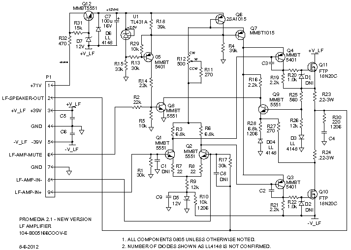
Schematic diagram of LF Amplifier Board
|
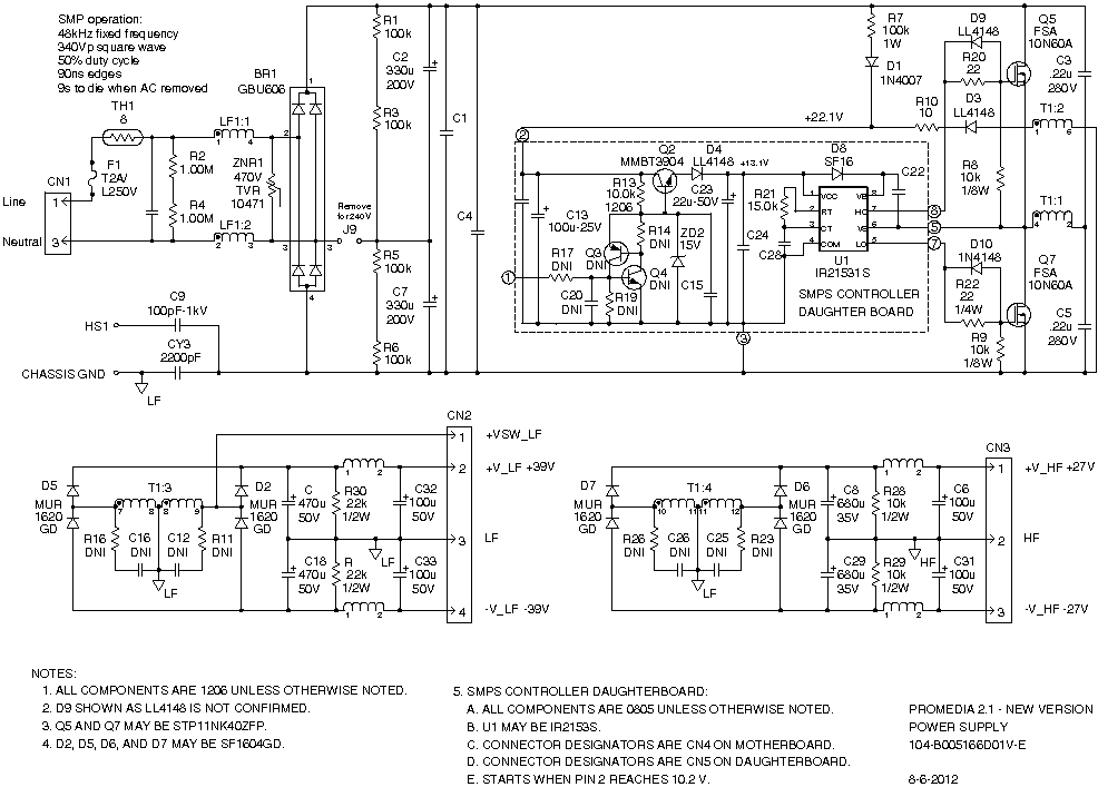
Switch-Mode Power Supply
The AC mains voltage passes through a small line filter and is then rectified to give approximately 340 Vdc for primary-high. Leaving off J9 configures BR1 for bridge rectification when the AC mains are 240Vac; stuffing J9 makes the bridge act as a voltage doubler when the AC mains are 120Vac, and gives the same approximately340Vdc. Primary-high is stored on a pair of series 200V electrolytic caps.
Resistor R7 and D1 deliver the initial voltage from primary-high to turn on the controller, U1, living on a daughterboard. Transistor Q2 and ZD2 form a discrete regulator to power the controller IC. Diode D4 prevents backwards current from flowing into the regulator. Once power is applied, U1 generates a 50% clock set by R21 and C28. Each clock state generates a high pulse on HO or LO, the isolated gate driver outputs, with a fixed deadtime inserted between pulses. This simply alternates turning on the two half-bridge transistors. Diode D8 and C22 form a bootstrap circuit to turn on the upper FET, recharging the cap when the lower FET is on.
The switched-mode power supply (SMPS) on the main SMPS board is a simple half-bridge, resonant, unregulated circuit. Each gate drive output goes through a gate resistor with ananti-parallel diode. The FETs, Q5 and Q7, alternately turn on, chargeing and dischargeing the transformer primary winding, T1:1. The resonant action of the supply is created because the current through the transformer primary must flow through either C3 or C5. This creates a square voltage waveform across the transformer primary with a sinusoidal current. This supply is very efficient as it uses zero current switching to (nearly) completely avoid switching losses. It's also excellent for audio applications because the lack of regulation isn't a detriment in the face of the high crest factor of audio signals. Finally, the square voltage waveform provides consistent, reliable output voltage.
During normal operation, T1:2 also gives a square voltage waveform which is rectified by D3 to supply the controller with operating voltage, relieving R7 of this duty.
Each secondary winding (T1:3 and T1:4) uses dual series rectifier diodes to bridge rectify the winding's voltage waveforms into a stable DC voltage. A small inductor filter reduces noise.
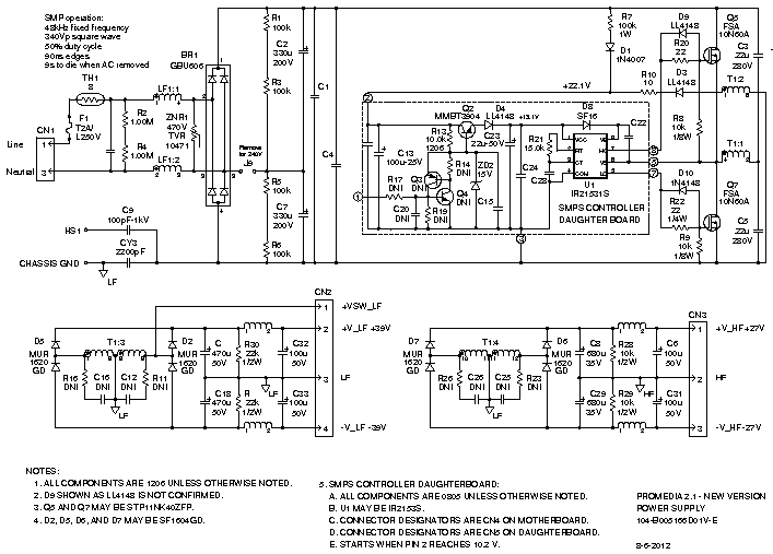
Schematic diagram of Switch-Mode Power Supply
|
Photo Gallery
_pic1_-90r-200x150.jpg)
View of backside of flatplate.
|
_pic2-200x150.jpg)
Major connectors.
|
Copyright Dale Thompson.
March 25, 2013 through
last revision on May 2, 2017
_pic1_-90r-850x638.jpg)
_pic2-850x638.jpg)