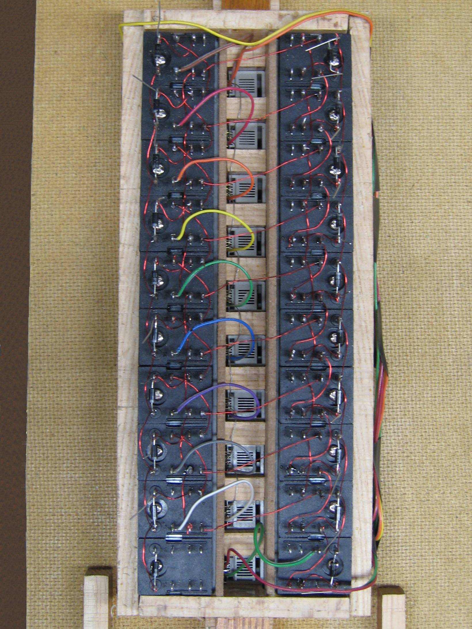
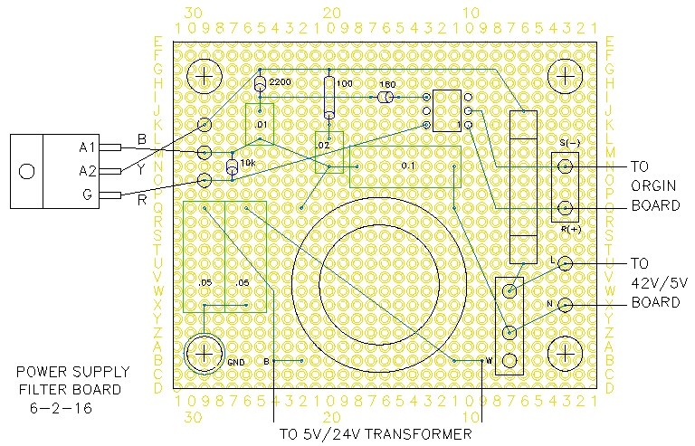
 Interconnect Diagram |
Circuitry is spread over four boards. The circuitry on the boards is not correlated 100% to that on the schematics, but is
close. Notice that letters between carots (>A>) are schematic-sheet-to-schematic-sheet points. Letters inside a circle are reference points on schematic sheets. I am sure this is confusing for anybody but me, but it was necessary for me to be able to keep track of the signals. |
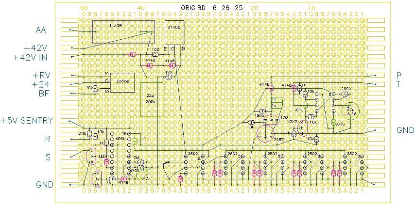
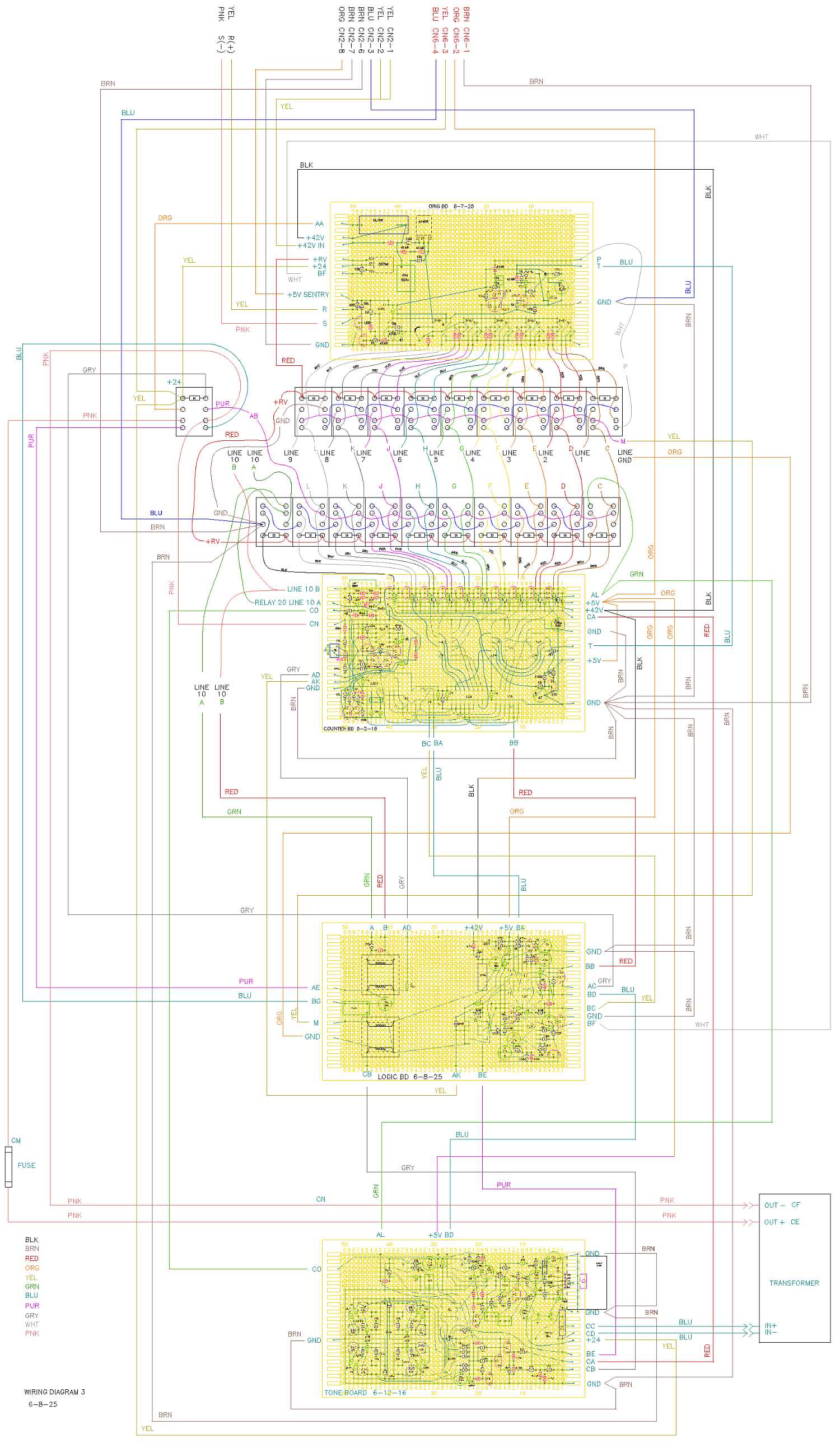
 Origination Relays Schematic Diagram |
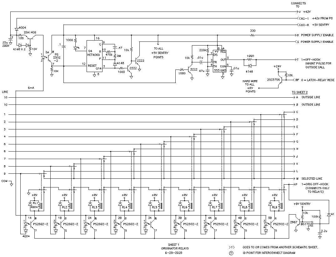
Line 10 >, outside line pass-through to A >. Line 10 >, outside line pass-through to B >. Line 1 > to Line 9 >, lines to local-exchange phones. Each line connected to an opto-transistor. When one phone goes off hook the other phones are locked out as originating phones. A > and B >, outside lines passed through to destination relays. C > to L >, local-exchange lines to destination relays. Pass local-exchange lines to destination relays except for one selected origination line. M >, line selected for origination phone. BF >, latch-relay reset. Normally floating high. Transistor open collector in control logic controls transistor that keeps +RV applied to relays. A low from transistor on control logic (sheet 2) turns off +RV and resets relays. +42V INPUT, continuously on from power supply. +42V, voltage following power-supply protecing diode and capacitor, powers opto-transistor diodes. +5V SENTRY, continuously on from power supply, keeps power-off, one-hour timer and off-hook timer powered when main power supply is off. +RV, relay power from transistor switch. R >, +5V SENTRY to main power opto-triac on sheet 5. S >, connection to main power opto-triac that is grounded by transistor to turn on main power when the phone goes off the hook. T >, origination-phone-is-off-hook, 6-second pulse to outside line answering logic. |
|
Optotransistor Biasing A simple current limiting resistor was originally used with the diodes of the optotransistors. Problems with getting the right current through the diodes due to the varying resistance of the old phones, and a problem with high current flow through the diodes on un-selected lines during ringing, resulted in a redesign. A 5mA constant-current source using a high-voltage PNP transistor solved both problems. A 150V transistor was used because it was available from a scrapped CRT monitor. A 200V transistor would give more margin as the peak voltage could reach 180V if the ring voltage was mis-adjusted above 70Vac to 90Vac. |
|
|
Relay Race There is a race condition when an origination phone goes off-hook. One relay is tripped, and the tripped relay should apply a ground to latch the selected relay. At the same time, the selected relay should remove the ground to the optocouplers for all other origination relays. But the relay is too slow. The origination relay is a break-before-make type, and does not reach the ground contact before the magnetic field collapses; the relay does not clamp. So, to stretch the ground presence long enough to let the relay latch, a time delay is needed. A 2N2897 transistor connecting the optocouplers to ground is normally biased on before any phone goes off-hook . When a phone goes off-hook the ground at pin P is removed, a clamping 1N4148 diode is disconnecteded, and the two-microfarad capacitor at the gate of a 2N170 MOSFET begins charging. This charging voltage rises until the MOSFET turns on, which turns off the 2N2897, which removes the ground to all the optocouplers. By that time, the selected relay has latched to a ground point. |
|
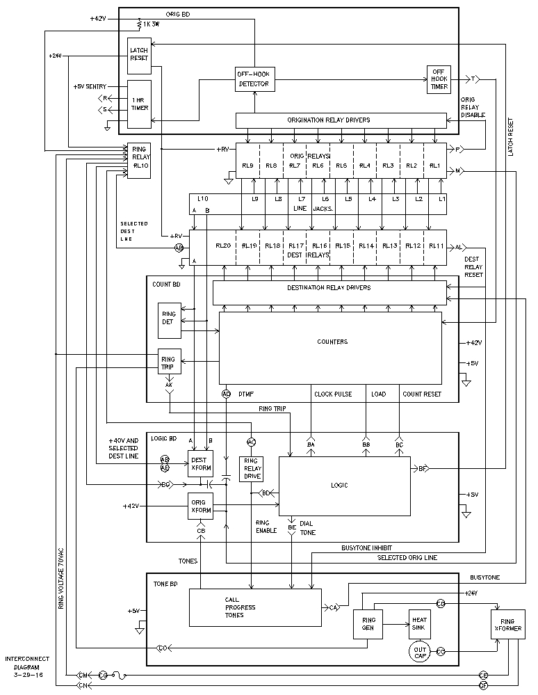
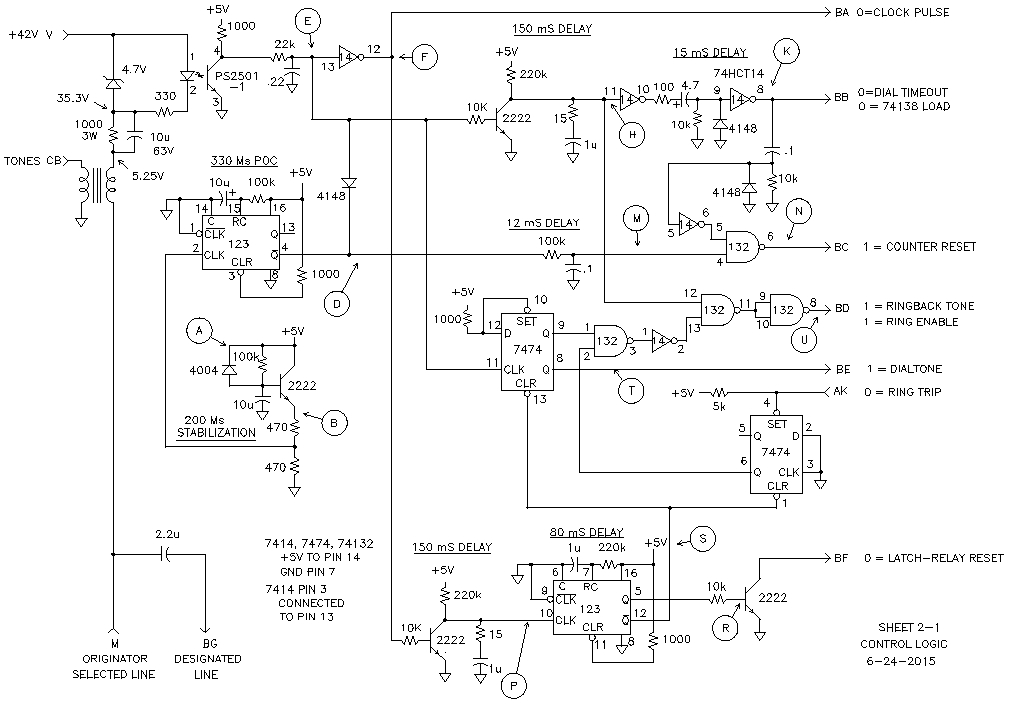 Control Logic Schematic Diagram |
200 ms stabilization circuit The 200-ms stabilization circuit provides about 200 ms delay after +5V is applied. This allows logic chips to power up and be in a fixed state before the power on clear (POC) At the end of the delay time, the POC circuitis clocked. 330 ms POC circuit One-half of a 74LS123 monostable flip-flop IC is used to set all critical logic chips to the starting state. The clock from the stabilization circuit is slow rising, but the Schmidt trigger clock input provides a clean switch. Call logic Timing of the control logic is initiated by the current through the transformer. Current from the +40V supply passes through the transformer and the selected telephone set. This current causes the PS 2502-1 opto-isolator to turn on. Refer to sheet 2-2 for the timing diagram. Latch reset When the origination telephone set goes on-hook (end of the call) for greater than 150 ms (remember a dial pulse is only 100 ms) the relays must be reset. The 150-ms delay circuit clocks the second half of the 74LS123 monostable flip-flop which produces a 80-ms pulse. The 74LS74 is reset and a low pulse at >BF is sent to the transistor on schematic sheet one that supplies +RV (+24V) to the relays. The previously selected relay is reset to its inactive position. Ring Enable One of the 74LS74 flip-flops is set when dialing begins. When dialing ends, ring-enable goes high. Upon ring-trip going low, the second 74LS74 flip-flop disables the ring-enable and prevents ring-enable from any further change until the latch-relay-reset occurs. |
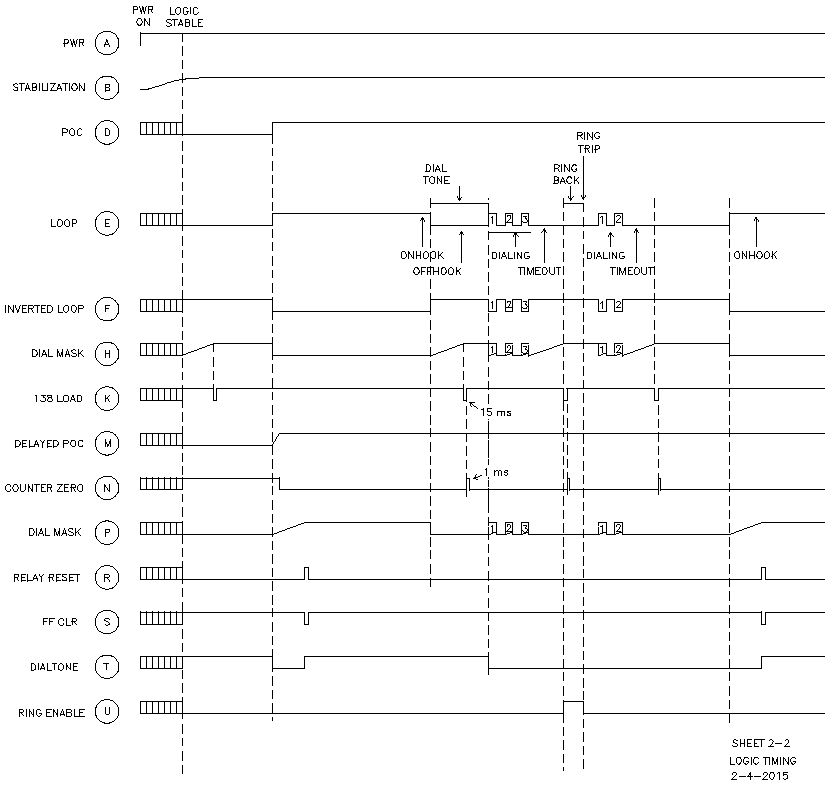 Control Logic Timing Diagram |
When the phone goes off-hook, the dial mask (H) starts charging, resulting in a 15-ms load pulse to zero the 74LS138 decoders. Dialing opens the phone loop at 10 pulses per second, and the opto-transistor supplies pulses to the logic circuits. The counter clock at >BA is applied to the 74LS93 counter. The time constant of the 150 ms dial mask (H) is longer than a phone dial pulse, and the dial mask is reset by each dial pulse. But, after the dial pulses stop (number is dialed) the dial mask level rises and initiates a 15-ms 74LS138 load pulse. The load pulse sets one of the destination relays, which locks out any further dial counting unless the line selected is the outside line (a dialing of a 0 , which is 10 pulses). The 74LS93 counter is set to zero by a 1-ms counter zero pulse (N) following the 15-ms 74 LS138 load pulse. If an outside line is selected, the control logic allows dialing an outside number, as the dialing pulses are now directed to the HT9200B DTMF chip. The 74 LS138 load pulse (K) now enables each DTMF tone before the counter is reset. The dial tone must only be produced before the first digit is dialed. The ring back tone must only be produced if the outside line number (0) is not dialed. A 74LS74 is used as a latch to inhibit the dial tone (T) as the first dial pulse is started. The ringback tone and ring enable (U) are activated after the dial tone stops and 150 ms after dialing stops. Ringtrip < AK from the counter board goes low when an inside phone is answered or an outside line is selected. The low at < AK forces the ringback tone / ring enable (H) to go low and inhibit both of them. |
|
Destination Relays Schematic Diagram |
A > to B >, relay normally connects to ring detector opto-transistor. A ring triggers the outside-line relay to connect the line to the transformer only if no other relay is already selected. Four NAND gates and three inverters enable the outside-line relay only in two scenarious: one, if the counter decoder (74138) is zero (no number dialed) and the 6-second, origination-phone-off-hook pulse is present, or two, if the selected line is 10. C > to L >, lines from originating relays that were not selected as the call origination line. Relay selects one-line as destination line. The remaining lines are connected to the busy tone through capacitors and to +40V through 10K-ohm resistors. +40V keeps the capacitors in the phones on the lines charged when not in use to prevent clicks and surges. T >, origination-phone-is-off-hook, 6-second pulse to answer outside line. CA >, busy signal tone. BA >, dial pulses to line-select counter. Triggers on the falling edge. BB >, load pulse to decoder latches line-select count and activates selected line relay. Triggers on falling BC >, counter reset. Resets on high and stays reset until reset goes low. BG >, audio output from destination transformer to origination transformer. BD< , high ring enable from logic board (sheet 2) turns on ring relay to connect ringer voltage and disconnect audio transformer. CM > and CN >, 70VAC sine wave from ring generator. AK >, ring trip held at +5V through 5K resistor until pulled low by 555 missing pulse detector or outside-line-select relay. AL >, busy tone inhibit. Stays at ground until a destination line is selected.. Ground turns on dialtone and ringtone emitter follower, and disables busy-tone emitter follower and 555 pulser.. When not grounded, the busy-tone emitter follower is enabled and the dialtone and ringtone emitter follower is disabled. |
Outside-Line Answering When an outside call occurs, it cannot be automatically answered or else the home phones not connected to the PBX would not be able to pickup the call. To allow both systems to pick up a call, the PBX must not connect to the outside line until a PBX phone is off hook. But if the PBX is in sleep mode (not having been used for an hour or more) there must be a delay after the phone is picked up before the PBX can connect to the outside line so that the logic circuits can stabilize. A 555 timer on the origination board senses when the origination phone goes off hook and holds an off-hook signal high for 6 seconds. This allows the logic on the destination board to stabilize, and also prevents a PBX phone from answering an outside call when a PBX-phone-to-PBX-phone connection is already in progress. The outside-line ring voltage turns on an opto-isolator transistor and discharges a capacitor. The capacitor voltage is monitored by a FET to keep a logic 1 at the 74LS132 gate during the non-ringing portion of the ring period. |
|
Ring Trip Ring trip has been reported as a major problem in home PBX designs, especially at a low frequency of 20 Hertz. The reports are true. Version 9 of the ring trip circuit here is not so simple but is reliable. SwitcherCad simulations show it will work with phones that have less than than 1000 ohms off-hook DC resistance. Old carbon transmitters in my phones ran from 150 ohms to 1800 ohms, so I had to do some phone repair before I could use some of them. But the repairs were needed anyway because the audio volume was low on those phones. There are two problems to be solved by a ring-trip circuit. One is to trip when the 20-Hz ring voltage drops due to the phone going off-hook, but not to trip when the 20-Hz ring voltage is ringing up to five bells. The second problem is to trip between rings when the DC voltage drops due to the phone going off-hook, but not to trip when the 20-Hz ring voltage drops the line voltage below the DC off-hook threshold. The AC portion of the ring trip circuit uses a 555 timer as a missing pulse detector, the missing pulse being the first ring voltage cycle excursion that is damped by the destination phone going off hook. The time period of the 555 is 36 milliseconds, so as long as the 555 is reset before 36ms the output at pin three of the 555 will stay high. Twenty Hertz is 50 ms; one half of that is the pulse detection time. First a few notes. DC voltage supplied to lines in my exchange is 42 volts. This circuit was designed for phone DC resistance up to 1000 ohms. Because my carbon transmitters were all over the map (150 ohms to 1800 ohms) I replaced most of the carbon transmitters with electret transmitters and now my phones are all under 350 ohms. My phones ring with 70 Vac, so that is what I use. I think this thing will work at other voltages. I modeled at 58Vac and 78Vac, but I did not test at other voltages. |
|
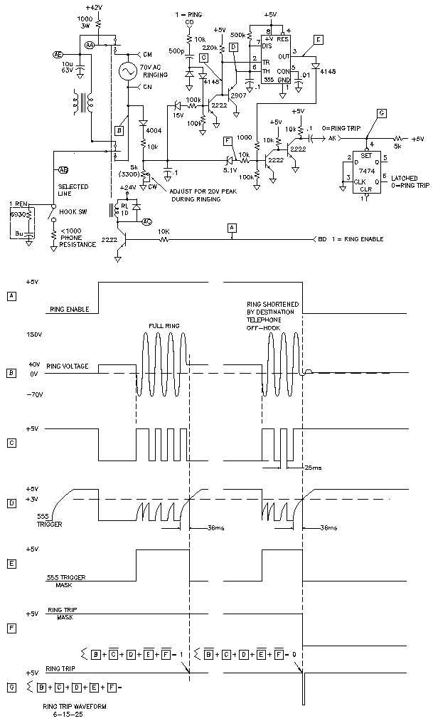 Ring Trip Diagram |
The 555 reset comes from the 70-Vac ring voltage, which goes from -58 to +142 volts ( +/-100 peak volts around the +42 Vdc voltage). The +142V excursion ring voltage is resistively divided down, breaks down the diode, 15V-Zener, and transistor barriers and causes a NPN-PNP transistor pair to produce the 555 reset pulse. The negative ring voltage excursion turns off the NPN-PNP pair and allows the 555 timing capacitor to begin charging. When the destination phone is picked, up the ring voltage is resistively divided by the 1000-ohm resistor and the less than 1000-ohm phone resistance to reduce the 142V excursion to less than the diode, 15V-Zener, and transistor barriers. If the barriers are not exceeded, there is no 555 reset, and the output goes low. The circuit operates as follows. Five volts for the 555 timer comes on when the origination phone is picked up. The 555 trigger is held high; not triggered. The 555 output is low, so when the threshold voltage rises to greater than +3 volts nothing happens; the 555 output remains low. When RING ENABLE at >BD> goes high and the ringing relay switches, +42 volts turns on the NPN-PNP transistor pair. The 555 timing capacitor is discharged, and the 555 is triggered. The 555 output goes high until the threshold voltage goes greater than +3 volts. Threshold voltage can't get above +3 volts because +42 V keeps the NPN-PNP transistor pair turned on, which keeps the threshold discharged. The negative excursion of the ring voltage cancels the +42 V and turns off the NPN-PNP pair. Threshold voltage rises, but it can't get to +3 V in 25 ms (555 monostable period is 36 ms). When the destination phone goes off hook, +42V and the +100 V peak voltage excursion are divided down to less than the 15V Zener barrier, so the NPN-PNP pair is not turned on and the threshold voltage rises above +3 volts, resulting in the 555 output going low. The high 555 output, is applied to the base of a NPN-NPN transistor pair where it blanks the DC line voltage monitor and prevents ring trip. Everything works fine unless the first ring voltage excursion is negative. The negative excursion would cause a false trip. To prevent a false trip, the RING signal that turns on the ring oscillator is used to trigger the first pulse of the 555 timer. The DC portion of the ring trip circuit uses a NPN-NPN transistor pair to monitor the DC line voltage. If the DC voltage is above the diode, 5.1V-Zener, and transistor barriers, the collector of the second NPN transistor is high. When the line voltage drops below the barrier threshold, the collector voltage drops. The high to low transition of the collector voltage, coupled through a capacitor to a 74LS74 set-input latches the ring trip. During the 20-Hz ringing period, the NPN-NPN pair is blanked by the 555 output applied to the first transistor's base. With the component values shown, and 5 ringers connected, SwitcherCad III predicts the trip will occur with a phone resistance of 1000 ohms or less and a ringer voltage of 80 to 110 volts peak (-38 to +142V peak-to-peak line voltage). With one ringer connected, SwitcherCad III predicts the trip will occur with a phone resistance of 1200 ohms or less and a ringer voltage of 110 volts peak (-68 to +152V peak-to-peak line voltage) , with a phone resistance of 1500 ohms or less and a ringer voltage of 100 volts peak (-58 to +142V peak-to-peak line voltage), or with a phone resistance of 2000 ohms or less and a ringer voltage of 80 volts peak (-38 to +122V peak-to-peak line voltage). |
 Audio and Ring Generator Schematic Diagram |
Audio tones are summed by 10K resistors, with a resistor to 2.5V bias. The bias connection keeps the sum point at 2.5V even when no tone is present so clicks aren't loud when ringback or busy tones are pulsed on and off. Emitter-follower output transistors have150 ohm resistors and 4.7V zeners to protect them from transients that may come back from the transformers or capacitors that they drive. 74HC4066 are HC and require a pull-up resistor to turn on. 74HCT4066 were not available at the foreign discount suppliers. The ring oscillator is a twin-tee that is turned off when ring trip goes low by shorting the 820-ohm resister to ground the collector of the oscillator. Transistor will go low so noise will not be amplified. The power amplifier is a single-chip amplifier driving a filament transformer in reverse. With a +24V supply it is capable of 7V rms, so a 1-to-10 transformer is needed. I used a 12V , 1A filament transformer. It has a 1-to-10 ratio and a 1-to-100 impedance ratio. A 600 ohm impedance transforms to 6-ohms, and is a good match for the amplifier chip. With the 10-ohm resistor added for short circuit protection, load impedance is about 12 ohms at the primary. For 7V rms output into 12 ohms, the current would be about 600 mA. |
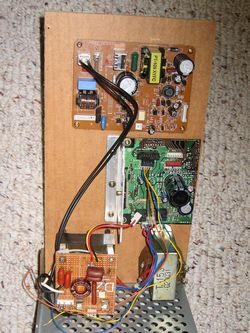
 Power Supply Schematic Diagram |
A switch-mode power supply from an Epson printer was in my junk box and is very energy efficient with no load. I used it to supply power to just the minimum number of components needed to wake up the rest of the components whenever one of the phones goes off-hook. The Epson supply just happens to have a +42Vdc output that I use to power the phone loop. When a phone goes off-hook, a logic signal from the origination board causes the TLP561J (MOC3041) opto-triac to turn on, which then turns on a BT139 triac. The +24V and +5V power supply (salvaged from another printer) has line-voltage power to it switched by the triac. A diode was added to the output from the +42V to prevent current backflow from the 70Vac, 20Hz ringing oscillator. This caused clipping of the negative swing of the ringing voltage. Addition of a 22uF, 200V capacitor following the diode restored the negative voltage swing. A 200V capacitor was used, even though a 160V one would have sufficed for a 70Vac ringing voltage. The extra margin was in case the oscillator was adjusted higher during setup, or I forgot that I was going to use 70Vac. |