Klipsch Promedia V4.1 Amplifier
Block Diagram
The BASH amplifier is not as complicated as it first appears. AC power of 117 volts is rectified to 156Vdc on the Input-Output board, and then goes to to the DC-to-DC converter. The converter drops the 156Vdc to +/- 30 Vdc that goes to 7815 and 7915 discrete IC regulators on the Input-Output board. From these regulators, the audio IC preamplifier stages get powered up. The converter also supplies a fixed 60-Vdc to what Indigo calls the Digital Converter.
The Digital Converter is the heart of the BASH amplifier. Voltage to the power amplifiers is kept just a few volts above the amplifier's output swing voltage by an audio processor hybrid pulse-width modulating a buck step-down converter. A buck step-down converter operates by applying short pulses of high voltage to an inductor in series with its output load. These pulses flow through the inductor, which builds a magnetic field. The collapse of the magnetic field between pulses keeps the current flowing at a constant rate into its load and back to the inductor through a diode. The voltage across the buck converter's load can be increased or decreased by changing the time the high voltage is applied to the inductor. Unlike the typical buck stepdown converter, in this design, the two FETs in parrallel that switch the high voltage are in the return path.
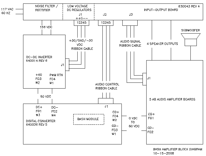
Block diagram of Indigo BASH amplifier in Klipsch Promedia V4.1
|
Below are the interconnections for the system. The control pod and the satellite speakers shown are separate units; all other connections are internal to the subwoofer box.
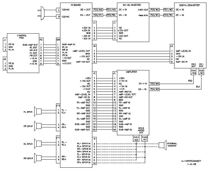
Interconnect diagram of Klipsch Promedia V4.1
|
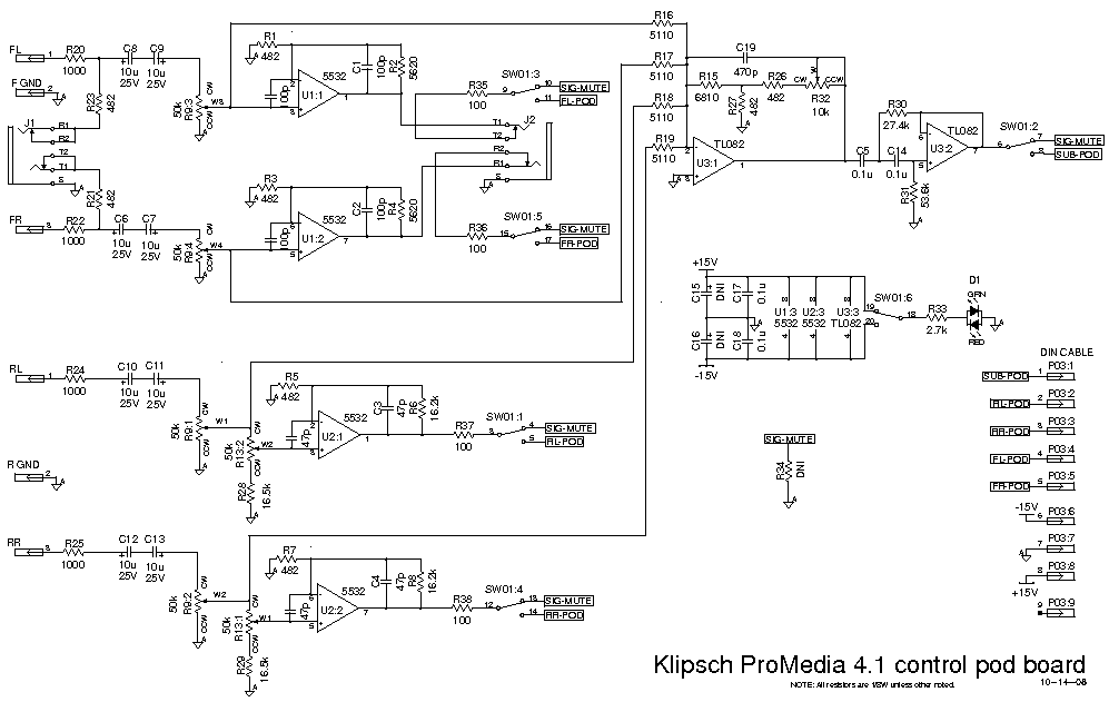
Control Pod
The control pod receives the left and right audio from the front and rear mini-jack inputs, provides an auxiliary input and headphone output, and mixes all four input signals into a summed subwoofer signal. All four audio inputs have their level controlled by a four-gang pot, and the surround channels have an additional cascaded two-gang pot for further level control. After buffering, the signal is sent to the I/O board through a DIN cable. The pre-buffer signals are also mixed together to create a subwoofer signal with level control, and are sent through a high-pass, second-order, Sallen-Key filter before leaving the control pod PCB. The front channel signal path is used for both the auxiliary input and headphone output. When headphones are plugged in, the signal is broken and the front-channel signal does not leave the control pod PCB.
The capacitors across the inputs of U1 and U2 are not part of the PCB, and are tacked onto the op-amp pins. It apparently helps eliminate oscillations. When the power switch is off, a bicolor LED is pulled to -15V and glows red, and all five output signals are pulled down to ground by R34, which isn't stuffed on the board. When the power switch is turned on, the bicolor LED is connected to +15V and is green. For the subwoofer channel, volume control is produced by changing the amount of feedback around an op-amp. Although it works, this is a poor design choice.
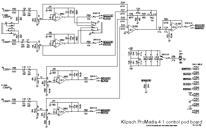
Schematic diagram of Control Pod
|
The DIN plug for the V2.400 and the V4.1 is an 8-pin, 45-degree-arc-per-pin, 270-degree-pin-arc-total plug. Its DIN specification is 45326 (obsolete specification replaced by IEC/DIN EN60130-9). When looking for a replacement, make sure it is the 270-degree version. Do not try to use the 8-pin plug with four, 45-degree arcs and two 41-degree arcs for a total pin arc of 262 degrees. The pin pattern in the 270-degree plug is a circle; the one in the 262-degree plug is horseshoe shaped.
The diagram below for the V4.1 DIN plug was taken from Klipsch forum postings that I believe is correct. I have not verified it, but I have not found any posts disputing its accuracy. The pin numbers on these diagrams don't conform to the DIN standard 45326.
The diagram for the V2.400 DIN plug comes from my own tracing of the wires on my plug. My control pod is the original unit, not the CP-1. I chose to identify the pins by using the pin numbers on the control pod circuit board connector.
These diagrams are shown looking at the mating side of the plug pins and not the soldered side.
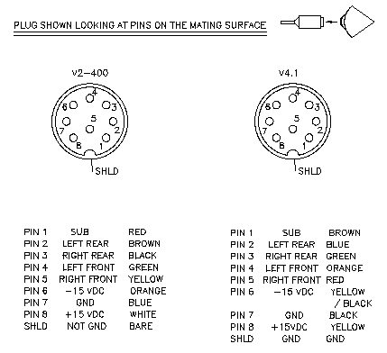
DIN Connector Wiring Diagram
|
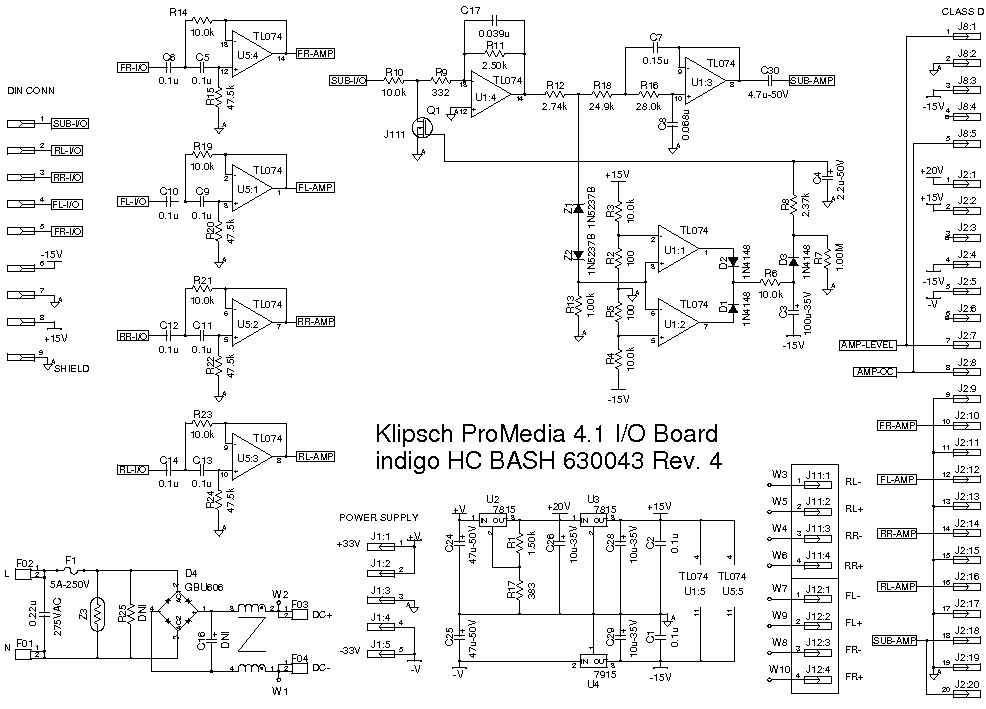
I/O Board
The I/O board performs many functions. Filtering for all five of the audio channels en route to the amplifiers, amplifier output connectors, housekeeping rectifiers, passive signal routing, and AC line rectification are all found here.
Voltage from the AC line is filtered, fused, and then rectified by D4. A common mode choke after the bridge rectifier helps block switching artifacts from the buck converter from making their way back to the AC line. Housekeeping voltage (in this case +/-33V; see DC-DC converter below) is sent to linear regulators to create a +20V and +/-15V regulated voltages. J1 and J8 are ribbon cables connecting to each respective power supply, while J2 is a ribbon cable going to the amplifier PCB.
Audio from the four satellite channels is received at the DIN connector, sent through a second-order, Sallen-Key, high-pass filter, and then passed to the power amplifiers. The subwoofer signal is buffered with a first-order roll-off, then sent through a second-order, low-pass, Sallen-Key filter. Finally, an AC coupling capacitor removes any DC offset. Between the two stages, the signal level is monitored by U1:1 and U1:2 acting as a bipolar window comparator. When the signal level approaches +/-9V (courtesy of Z1 and Z2), the comparators trip and pull high. C3 and C4 are charged until the gate threshold for Q1 is reached and the subwoofer audio signal is pulled to ground (effectively muting the subwoofer). R7 then slowly discharges C3 and C4 until D3 becomes reverse biased, at which point only C4 is discharged. By that time, Q1's gate is below the threshold and the subwoofer signal is re-enabled. J11 and J12 are spring clip outputs for the 4 satellite speakers.
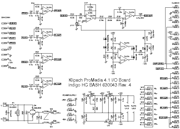
Schematic diagram of I/O Board
|
Digital Converter
The Promedia V4.1 uses a Class G "tracking" output stage (Class H outside of the US), which means that the rail voltage of the amplifier is held slightly higher than the level required to reproduce the audio signal. This reduces dissipation in the amplifier output stage greatly because the amplifier is only required to reproduce high output power for small amounts of time - most of the time the power required by the speakers to reproduce audio is very small. The rail-voltage tracking power supply is simply a cleverly re-arranged buck converter with the inductor and switches in the return leg instead of the supply leg. This has the benefit of allowing ground-referenced, N-channel FETs to be used with simple, resistive current sensing. The disadvantage is that the feedback signal must be re-referenced from the output ground (which is circuit ground) to the input ground (floating with respect to circuit ground). The operation of a buck converter is covered extensively at many online sources.
It is worth noting that current is sensed in only one of the FETs, meaning the converter relies on good matching of the FETs both electrically and thermally for protection from current hogging. Since FETs have a negative temperature coefficient , this is a reasonable tradeoff for a consumer product since it eliminates having to measure and combine the current from two parallel switches and provide protection for each switch separately. The 55V FETs seem to be in danger in a 60V nominal, 53V measured, circuit, but loading of the unregulated DC-DC converter and unavoidable voltage losses in the system (such as the current sense resistors) apparently keep the devices from failing. It is my belief that there is insufficient margin, but Klipsch must have felt otherwise. A ferrite bead (FB1) is used to eliminate spikes on D6, thus reducing dissipation and recovery time. C4, the output capacitor, is a large film cap instead of the traditional electrolytic - this provides a low output impedance of the supply for the amplifier. MTG1 is a mounting stud that screws to the mounting plate, and is shown on the schematic because it had the
connections to C14 and C15.
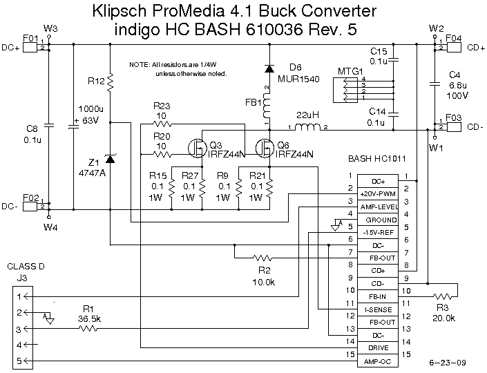
Schematic diagram of Digital Converter
|
Indigo BASH HC1011 Module
The HC1010 or HC1011 Module uses a UC3842A controller IC to drive the FETs in the Digital Converter in response to the demands fed to it by the Amplifier Board's AMP-LEVEL signal. A current threshold is established in the UC3842A by the AMP-LEVEL signal. Feedback of the rail voltage to the Amplifier Board at FB-IN reduces the threshold when the rail votage approaches the established point. In the UC3842A, the threshold sets the point where the I-SENSE voltage from the Digital Converter FET source resistor will cause the UC3842A to cut off the DRIVE output to the FET gates. Switching off the FET gate drive determines the pulse width of the buck converter in the Digital Converter, and in turn establishes the Amplifier Board rail voltage.
An AMP-OC circuit is incorporated in the Module that reduces the rail voltage if excessive current is being drawn by any of the Amplifier Boards.
For a more detailed description of the Module operation click here.

Schematic diagram of Indigo BASH HC1010 / HC1011 Module
|
Module Versions
Some early V4.1 units may have used an HC1010 module instead of the HC1011, or perhaps some of the late V2-400 used the HC1011. The change over date is not known.
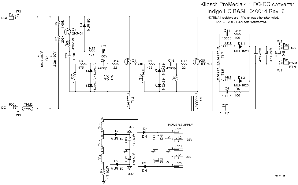
DC to DC Converter
To isolate the AC line from the rest of the system, a self-oscillating push-pull converter is used as an ideal transformer. The rectified line voltage, from the I/O board, is transformed by roughly one-third and galvanically isolated to create a unipolar main rail for the buck converter of approximately +53V. THM2 is an NTC which presents a low resistance to limit inrush upon startup, but the resistance drops as it heats up so the NTC has little effect once the supply is running. R5 and R7 divide the AC line voltage so that Q1 turns on at about 100VAC and Q7 avalanches. This turns on Q4 and the supply begins oscillating. Turning on one switch turns on the other switch the next cycle, and thus the supply is self-oscillating. Because of the operation of a push-pull supply, the voltage stress is high on the switches which is a hindrance because high voltage switches must be used. However, at this relatively low power level it's not a big issue. The secondary is full-wave rectified with ferrite beads in series with the rectifiers and snubbers across them. C27 provides a path for high-frequency switching currents to return to the source, likely helping the amplifier module to meet emissions requirements. The operation of this converter is covered in US patent US6108219.
The auxiliary voltages (+/-15) are created using a single winding (driven bipolar by the primary) that is full wave rectified to create bipolar rails. Although two windings are available to create slightly different voltages and allow a selection of auxiliary voltages (since either output feeds the same regulators on the I/O board) only one of the two supply parts are stuffed (DNI on the schematic means 'do not insert'). The transformer windings used provide about +/-33V. While the auxiliary voltage is referenced to circuit ground, the buck converter's specific implementation means the main output is not ground referenced until the output of the buck converter.
To address possible failures the DC-DC converter has ferrite beads in series with the auxiliary windings. The series resistor, R27, seems to be undersized as it was discolored on my board and failed. Discolorization was also noted on R1 and R2 but they both measured the correct value.
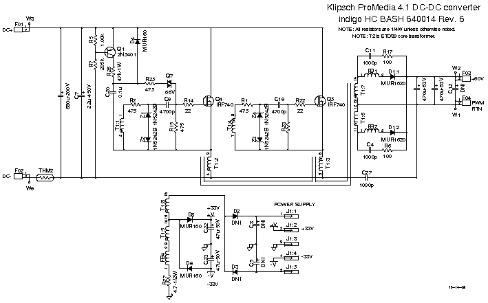
Schematic diagram of DC to DC Converter
|
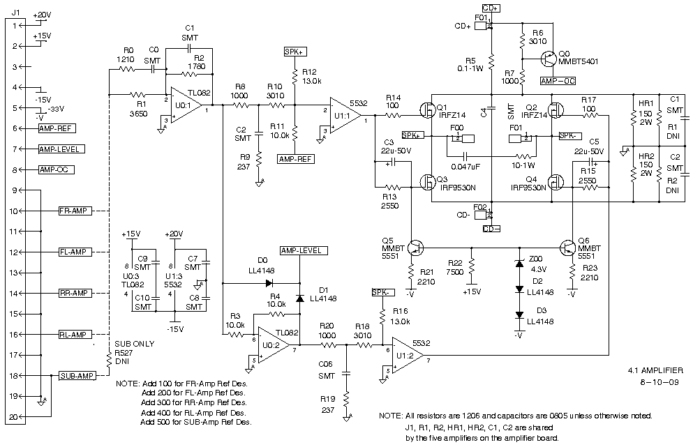
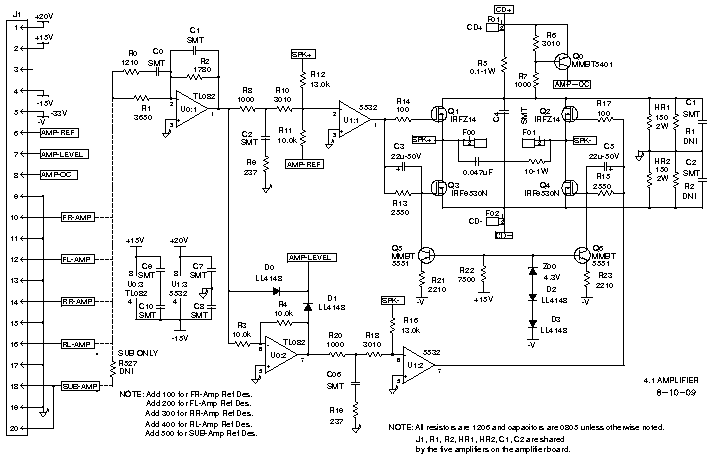
Amplifier Board
All five amplifiers are on the same PCB and use SMT parts. Only one channel is shown but all parts except for HR1, HR2, R1, R2, C1, C2, and R527 are repeated for each channel (see the schematic note about reference designators). The amplifier topology is linear full bridge. Audio is received, filtered, and buffered by U0:1. Only the subwoofer channel only R527, which is unconnected on one side but still stuffed on the PCB. The audio signal from U0:1 is then inverted by U0:2. The non-inverted and inverted audio signals are rectified by D1 and D0, and connected with all the other amplifier channel's audio signals to form an AMP-LEVEL voltage. The combined AMP-LEVEL voltage tells the buck converter how high the amplifier rail voltage needs to be to allow the amplifier with the greatest audio signal to reproduce that audio signal. The bifurcated audio signals are filtered and mixed with feedback by both gates of U1, which drives the output FETs. R11 connects one polarity of the audio signal of all channels together. The upper FET, and N-channel, is driven directly by the op amp. The lower P-channel FET is capacitively driven with a DC-restoring network on the gate side of the capacitor.
HR1 and HR2 are used to load the buck converter and have parallel SMT resistors, which are not stuffed (R1 and R2). R5 for each channel measures the current flowing to the output stage. When output current reaches a threshold of about 9A, Q0 pulls the collector high and notifies the buck converter that an overcurrent condition exists on one channel. Any channel experiencing overcurrent will trigger shutdown of the entire supply.
Due to the inherent danger in destroying SMT parts, no capacitors were removed for measurement and have "SMT" instead of their capacitance value shown.
Schematic diagram of Amplifier Board
|
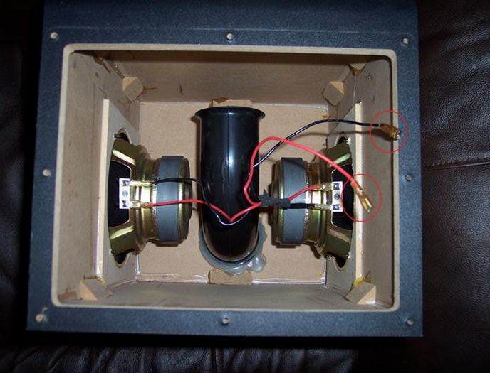
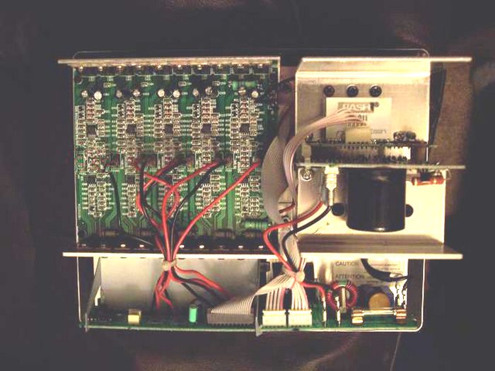
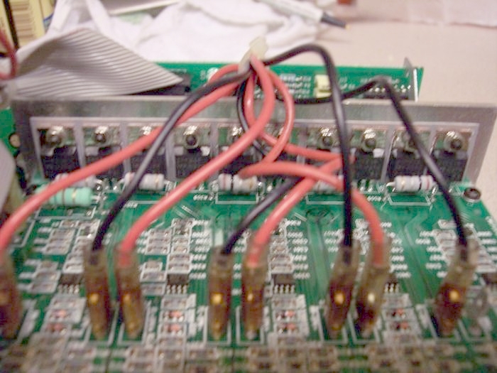
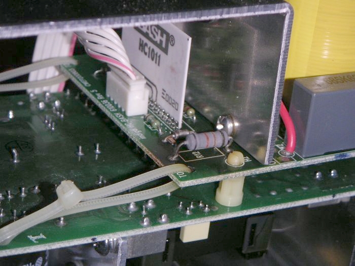
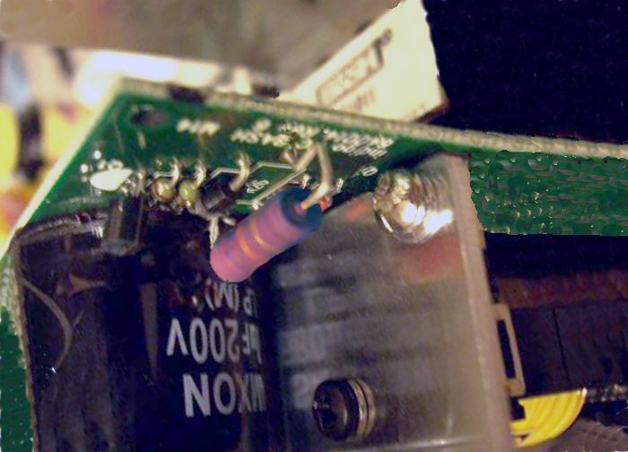
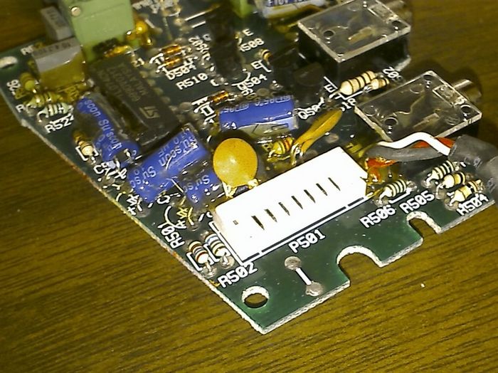
Photo Gallery
Copyright Dale Thompson.
September 10, 2008 through
last revision on August 11, 2009